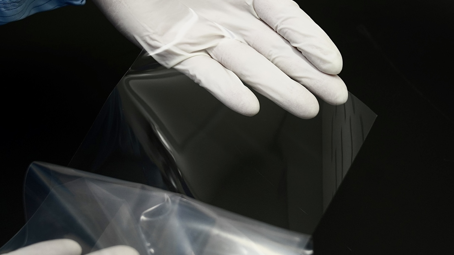
Fluorokey’s Pyflon™ fluoropolymer platform offers an ultra-low refractive index (n ≈ 1.29), broadband transparency (200–2000 nm), and exceptionally low optical loss (<0.1 dB/cm), positioning it as a next-generation cladding and waveguide encapsulation material for silicon, silicon nitride, and indium phosphide photonic systems.
Unlike conventional inorganic oxides, Pyflon™ provides superior mechanical flexibility, chemical stability, and plasma-etch compatibility, enabling conformal deposition over complex 3D photonic structures without introducing microvoids or stress-induced birefringence. Its amorphous molecular structure minimizes optical scattering and surface states, while maintaining a high glass transition temperature (>200 °C) for robust thermal endurance in wafer-level processing.
Pyflon™’s optical isotropy and dielectric uniformity also support emerging co-packaged optics (CPO) and silicon photonics interposers — key technologies for next-generation AI data centers and neuromorphic accelerators. The material’s gas-permeable yet moisture-resistant characteristics allow fine environmental control for encapsulated photonic cavities and resonators, ensuring long-term wavelength stability.
Through deep collaboration with partners in the photonics and semiconductor industries, Fluorokey is pioneering a new material integration route, enabling low-loss optical interconnects, on-chip modulators, and hybrid photonic packaging — laying the material foundation for light-speed AI infrastructure.